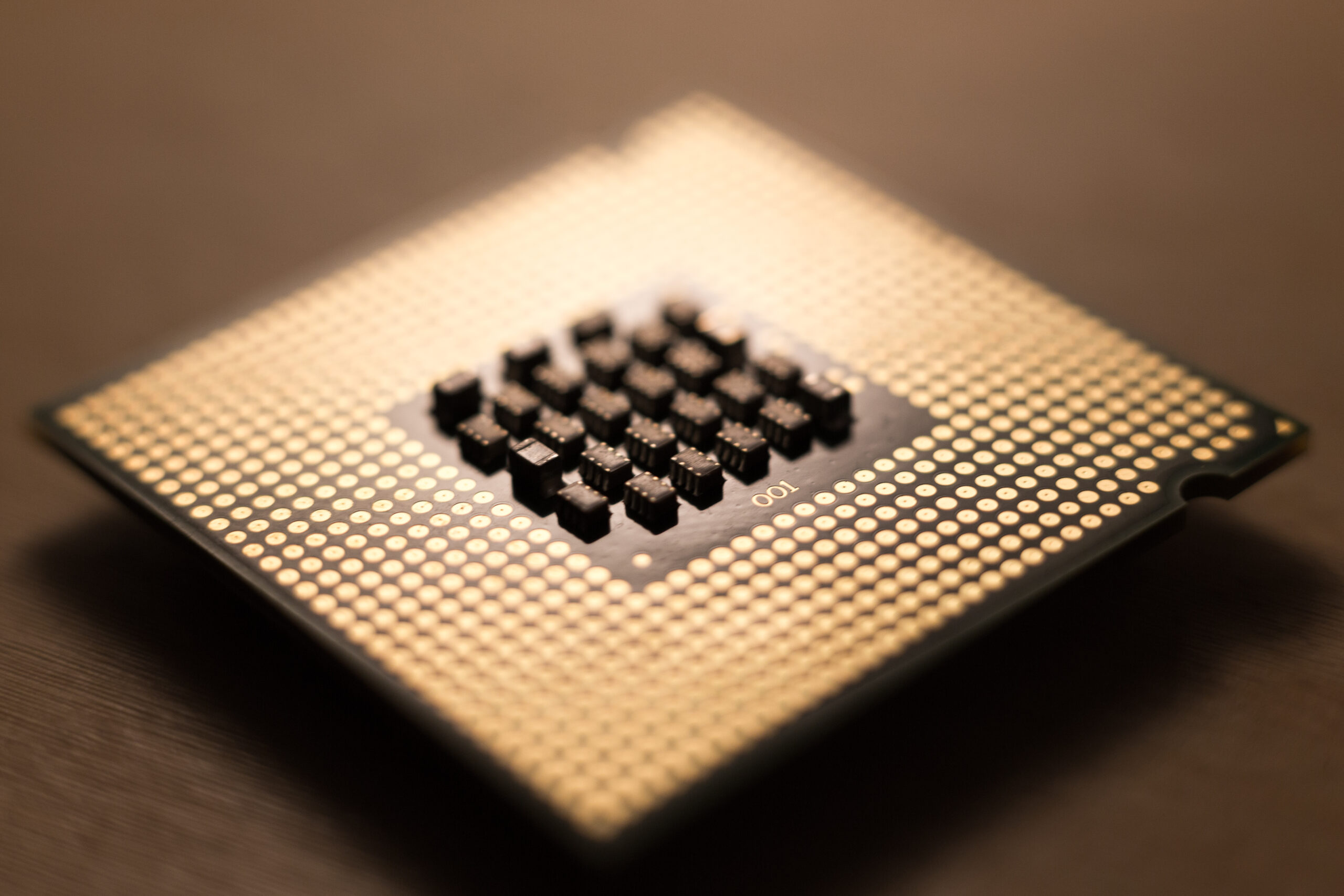
Silicon wafers are the foundational substrate used in the fabrication of semiconductor devices, serving as the canvas upon which complex electronic circuits and components are constructed. The process of silicon wafer processing involves a sequence of precise steps that transform raw silicon into intricately patterned structures capable of performing advanced electronic functions. Here’s a comprehensive overview of how silicon wafers are processed.
1. Wafer Formation:
- Starting Material: High-purity silicon is derived from metallurgical-grade silicon through a refining process that achieves purity levels of 99.9999% (6N) or higher. This silicon is typically sourced from quartzite or sand.
- Silicon Ingot Growth: The purified silicon is melted in a crucible and then slowly cooled while being pulled upwards to form a single crystal ingot. This process, known as the Czochralski method, ensures the crystal structure is aligned in a uniform direction, crucial for semiconductor performance.
- Wafer Slicing: Once grown, the silicon ingot is sliced into thin, circular discs called wafers using diamond saws. These wafers are typically between 150mm to 300mm in diameter and are polished to achieve a smooth, defect-free surface.
2. Wafer Cleaning and Preparation:
- Cleaning: Wafers undergo extensive cleaning processes to remove contaminants, particles, and residues that could adversely affect semiconductor device performance. This cleaning is performed using ultrapure water, chemicals, and sometimes involves techniques like megasonic cleaning to ensure cleanliness at the nanometre scale.
- Surface Preparation: After cleaning, wafers undergo surface preparation steps such as etching or chemical mechanical polishing (CMP) to achieve a pristine surface with minimal roughness and defect density. This smooth surface is crucial for subsequent processing steps.
3. Thin Film Deposition:
- Purpose: Various materials, including silicon dioxide (SiO₂), silicon nitride (Si₃N₄), and metals (such as aluminium or copper), are deposited onto the wafer’s surface to form thin films. These films serve as insulators, conductors, or protective layers in the semiconductor device.
- Deposition Techniques: Common methods include chemical vapor deposition (CVD), physical vapor deposition (PVD), and atomic layer deposition (ALD), each chosen based on the specific material properties and desired film thickness.
4. Photolithography:
- Pattern Definition: Photolithography is used to transfer intricate patterns and designs onto the wafer’s surface, defining the layout of semiconductor components.
- Steps Involved:
- Photoresist Coating: A photoresist material is applied uniformly over the wafer.
- Exposure: The wafer is exposed to ultraviolet (UV) light through a photomask, which contains the desired circuit pattern.
- Development: Chemicals are used to selectively remove either the exposed (positive photoresist) or unexposed (negative photoresist) areas of the photoresist, exposing the underlying wafer material.
5. Etching:
- Pattern Transfer: Etching processes are employed to selectively remove material from the wafer according to the pattern defined by the photoresist.
- Types of Etching: Wet etching uses liquid chemicals to dissolve and remove materials, while dry etching (plasma etching) utilizes reactive gases and plasma to achieve higher precision and control over the etching process.
6. Doping:
- Introduction of Dopants: Dopant atoms, such as phosphorus or boron, are introduced into specific regions of the silicon wafer to modify its electrical properties. This process is critical for creating n-type and p-type semiconductor regions essential for transistor operation.
- Ion Implantation: High-energy ions are accelerated and implanted into the wafer’s surface to precisely control the depth and distribution of dopants within the semiconductor material.
7. Oxidation and Annealing:
- Oxidation: Thermal oxidation processes grow silicon dioxide (SiO₂) layers on the wafer’s surface, serving as electrical insulators and protective barriers.
- Annealing: Heat treatments (thermal annealing) are applied to activate dopants, repair crystal lattice damage caused by ion implantation, and optimize the electrical characteristics of the semiconductor devices.
8. Metallization and Interconnection:
- Metal Layer Deposition: Thin layers of metals (e.g., aluminium, copper) are deposited onto the wafer’s surface to create electrical contacts and interconnects between different semiconductor components.
- Patterning: Photolithography and etching processes define the precise locations and shapes of metal interconnects, ensuring reliable electrical connections and signal propagation across the semiconductor device.
9. Dielectric Deposition and Passivation:
- Dielectric Layers: Insulating materials such as silicon nitride (Si₃N₄) and additional layers of silicon dioxide (SiO₂) are deposited to isolate and protect semiconductor components from electrical interference.
- Passivation: Surface passivation techniques form protective layers that enhance device reliability by preventing moisture ingress, chemical contamination, and mechanical stress.
10. Testing and Quality Control:
- Electrical Testing: Each wafer undergoes rigorous testing to evaluate its electrical characteristics, functionality, and performance under simulated operating conditions.
- Defect Inspection: Advanced inspection tools, including scanning electron microscopy (SEM) and optical inspection systems, detect and analyze defects that could impact semiconductor device reliability and yield.
11. Packaging and Assembly:
- Wafer Dicing: Wafers are diced into individual semiconductor devices (chips) containing the fabricated circuits and components.
- Packaging: Each chip is mounted onto a package substrate and connected to external leads or pins through wire bonding or flip-chip bonding techniques.
- Encapsulation: Chips are encapsulated in protective materials (e.g., epoxy resin) to safeguard against environmental factors, mechanical stress, and physical damage.
12. Final Testing and Yield Optimization:
- Functional Testing: Packaged semiconductor devices undergo final electrical testing to verify their functionality, performance, and reliability according to industry standards.
- Yield Enhancement: Statistical process control (SPC) methodologies and yield optimization strategies are employed to maximize the number of defect-free semiconductor devices per wafer, ensuring high manufacturing yield and cost-effectiveness.
Advanced Technologies and Future Directions:
- Advanced Materials: Exploration of new semiconductor materials (e.g., gallium nitride, silicon carbide) with superior electrical properties for enhanced device performance and efficiency.
- Nanotechnology: Advancements in nanoscale fabrication techniques facilitate the production of smaller, more energy-efficient semiconductor devices with increased functionality and integration density.
In conclusion, silicon wafer processing is a meticulously controlled and sophisticated series of steps that culminate in the creation of high-performance semiconductor devices. This process integrates scientific principles with advanced engineering techniques to meet the demands of modern electronics, driving innovation and technological progress across various industries.


